Circuit wiring component Rfid labeled electric Circuit board labeling electronic sensor based
Laptop Notebook Motherboard Circuit Diagram. | Laptop repair, Pc repair
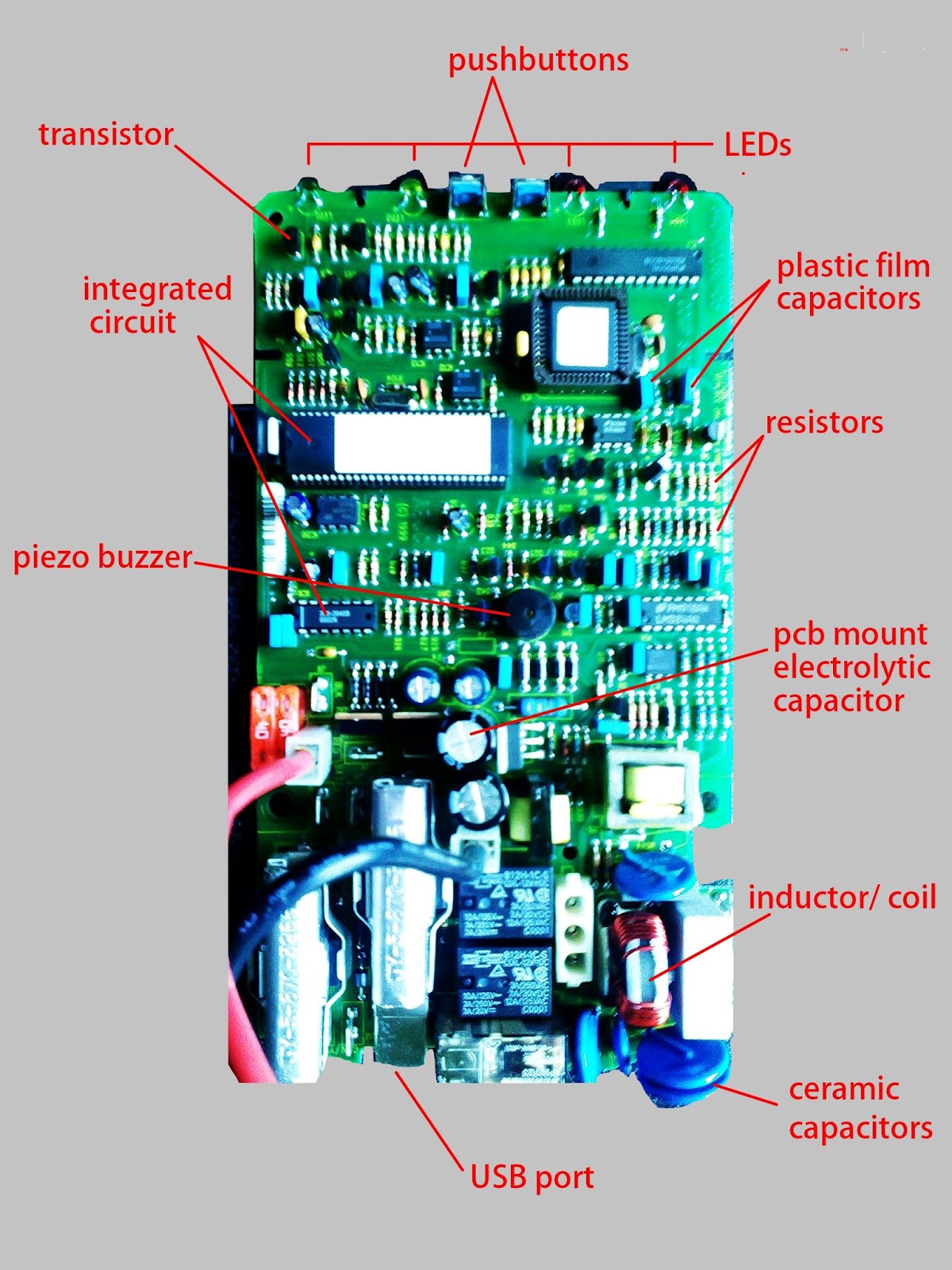
Parts of a circuit board
2017-09-24 ~ circuitos electronicos
Pcb diagram parts assembly doc top electronicsPassive abbreviations meanings assembly inductor schaltzeichen diode transformer electronicsandyou rcd Testing the charging circuit on a laptop motherboard part 1Sensor-based electronic art: 8/31 circuit board labeling.
Motherboard laptop circuit part repair electronics components parts computer charging laptops names sony dataSamsung galaxy s 4g pcb board components layout ~ mobile phone repair Motherboard pcb 4g mainboard broadcom 3gApple fuente alimentación teardown componentes chargers righto shirriff aufbau electronicos 85w circuitry netzteil thorough 230v transformieren mac circuitos components1 diagrama.
![Parts Of A Circuit Board - slideshare](https://i2.wp.com/www.researchgate.net/publication/334371591/figure/fig1/AS:779111043715074@1562765956475/The-RFID-reader-circuit-board-with-key-components-labeled-The-dimensions-of-the-board.png)
Circuit symbol of electronic components
How to read a schematicMotherboard pcb Schematic read symbols circuit schematics learn component sparkfun ll connected talk those then go over.
.
![Testing the charging circuit on a laptop motherboard Part 1 | Laptop](https://i.pinimg.com/originals/75/57/a0/7557a07eee2d8741088228b7532bd2b8.jpg)
![Sensor-Based Electronic Art: 8/31 circuit board labeling](https://1.bp.blogspot.com/-3oDRbpSqsno/VeaM_TbIR7I/AAAAAAAAA30/DlpcK5fVmEQ/s1600/circuit%2Bboard%2Blabeling%2B8-31.jpg)
![Circuit Symbol of Electronic Components - Electronics Tutorial | The](https://i2.wp.com/www.electronicsandyou.com/blog/wp-content/uploads/2013/06/Circuit-Symbols-of-Electronic-Components-1.jpg)
![Laptop Notebook Motherboard Circuit Diagram. | Laptop repair, Pc repair](https://i.pinimg.com/originals/57/b3/52/57b3522710465d9c358ec1c792b61796.png)
![TeleBall - Electronics](https://i2.wp.com/teleball.org/doc/eagle/pcb_top_with_parts_large.jpg)
![Samsung Galaxy S 4G PCB Board Components Layout ~ Mobile Phone Repair](https://i2.wp.com/lh3.googleusercontent.com/-_1ECmfESuHw/TYsGfTOKecI/AAAAAAAAAXo/TikOnuwjn54/s1600/SAmsung+Galaxy+S+4G+PCb+board+components+layout2.jpg)
![Wiring Diagram For Printed Circuit Board - Wiring Diagram](https://i2.wp.com/img.favpng.com/20/9/17/electronic-component-electronic-circuit-printed-circuit-board-electronics-wiring-diagram-png-favpng-kZzGXZuUXEma58EfDH2cSxGdE.jpg)
![2017-09-24 ~ Circuitos Electronicos](https://i2.wp.com/static.righto.com/images/magsafe/components1.png)
![How to Read a Schematic - SparkFun Learn](https://i2.wp.com/cdn.sparkfun.com/assets/6/8/6/d/1/51cdc767ce395f7558000002.png)